■工学部_研究紹介_2017_英語版ファイル161220
24/80
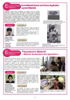
Piezoelectricmaterialisusedasanultrasonictransducerandanignitionelementoflighter.Thematerialgenerateselectricity(electriccharges)whenpressureisapplied,anditdeforms(expandsandcontracts)whenavoltageisappliedonthecontrary.Sincemanyofpiezoelectricceramicsusednowcontainharmfullead,thereisanincreasingdemandforlead-freepiezoelectricmaterials.Thereforeweconductresearchonsuchlead-freepiezoelectricceramics.Furthermore,weareapplyingpiezoelectricceramicstodevelopultrasonicmotors.Piezoelectricmaterialcanconvertkineticenergy(pressure,displacement)andelectricalenergy,thusisappliednotonlytoasensorbuttoavibratorandanactuator.Sincetheirperformancesdependonthecharacteristicsofthematerial,itisimportanttodoresearchonthematerialdevelopment.Besides,thedevelopmentofpiezoelectricmaterialrequiresanewdevice.Ourstudentsworkhardtoexploreanewmaterialanditsapplication.NorikoBambaAssociateProfessorI worked at ShinshuUniversity after received the Ph.D. (Engineering) in Materials Chemistry atOsakaUniversityin1998.Researchfield:・electronicmaterialsMakepiezoelectricceramics.Powderwaspressedintoapelletusingthispressingmachineandfiredatabove1000oC,thenceramicswasobtained.Piezoelectric Material ~Material development and application~Characterizationoftheceramics.Thedielectricconstantorresonancepropertyaremeasuredwithchangingtemperatureorfrequency.Ourgraduatesareworkingatelectricpowdercompaniesandhomeelectricsmakersoraspublicofficials.Iamteachinghowtocarryouttheresearchandsolveproblemsthroughtheresearch,sothatthestudentswillsucceedinplayinanyfields.BambaLabIn the FutureAfter GraduationElectrical& Computer EngineeringWehavetostudysemiconductormaterialsanddevices.Andmanufacturalequipmenthastobeoperatedandmaintainbyyourself.Youcanbeactiveinvariousfieldofelectricalmanufacturer,materialsandequipment.Integratedcircuits(ICs)technologyarewidelyusedfortoday’sinformationsociety.However,highspeedcalculationandprocessinghavebeendemandedyearafteryear.Asthemoment,consistingdevices(LSIs)fortheICchipsisminiaturizationandtheincreaseofthedevicenumber.Essentialsolutionisnecessaryfortheissuebecauseminiaturizationisreachedatomicsize.Inordertosolvetheproblem,theintroductionofhighmobilitymaterialsand/oropticalcommunicationhavebeenproposed.Layeredmaterialsincludinggrapheneandtransitionmetaldichalcogenidehavereceivedmuchattentionfornoveloptoelectronicmaterials.Layeredmaterialshavebeenreceivedmuchattentionbecauseofgraphenestudy.Forlayeredmaterials,theformationofhighqualitycrystalsareoneofimportantissue,andtheissueisdifficult.Inaddition,Iamstudyingnovelmaterialswithlarge-scaleformation,whichareimportantforlayeredmaterials.Inthislaboratory,researchresultshavebeendisseminatedtotheworld.NoriyukiUrakamiAssistant ProfessorPh.D.(Engineering) Toyohashi University of technology. Research topics ・Semiconductor・Crystal growth,・Optoelectronics・Layered materialNovel Material Searchand Device ApplicationLayered MaterialsUrakamiLab.In the FutureAfter GraduationElectrical& Computer EngineeringMolecularbeamepitaxy.Thisapparatuscanbeusedforanepitaxialgrowth,whichdegreeofvacuumismaintainedto10-7Pa.Layeredmaterials;Molybdenumdisulfide(MoS2)flake.MoS2showthepropertyinsemiconductor.MoS2hasbeenexpectedtonext-generationoptoelectronicmaterials.22
元のページ