Engineering-Research-Activity2016|SHINSHU UNIV.
24/80
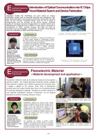
Piezoelectricmaterialisusedasanultrasonictransducerandanignitionelementoflighter.Thematerialgenerateselectricity(electriccharges)whenpressureisapplied,anditdeforms(expandsandcontracts)whenavoltageisappliedonthecontrary.Sincemanyofpiezoelectricceramicsusednowcontainharmfullead,thereisanincreasingdemandforlead-freepiezoelectricmaterials.Thereforeweconductresearchonsuchlead-freepiezoelectricceramics.Furthermore,weareapplyingpiezoelectricceramicstodevelopultrasonicmotors.Piezoelectricmaterialcanconvertkineticenergy(pressure,displacement)andelectricalenergy,thusisappliednotonlytoasensorbuttoavibratorandanactuator.Sincetheirperformancesdependonthecharacteristicsofthematerial,itisimportanttodoresearchonthematerialdevelopment.Besides,thedevelopmentofpiezoelectricmaterialrequiresanewdevice.Ourstudentsworkhardtoexploreanewmaterialanditsapplication.NorikoBambaAssociateProfessorI worked at ShinshuUniversity after received the Ph.D. (Engineering) in Materials Chemistry atOsakaUniversityin1998.Researchfield:・electronicmaterialsMakepiezoelectricceramics.Powderwaspressedintoapelletusingthispressingmachineandfiredatabove1000oC,thenceramicswasobtained.Piezoelectric Material ~Material development and application~Characterizationoftheceramics.Thedielectricconstantorresonancepropertyaremeasuredwithchangingtemperatureorfrequency.Ourgraduatesareworkingatelectricpowdercompaniesandhomeelectricsmakersoraspublicofficials.Iamteachinghowtocarryouttheresearchandsolveproblemsthroughtheresearch,sothatthestudentswillsucceedinplayinanyfields.BambaLabElectrical& ElectronicEngineeringIn the FutureAfter GraduationWehavetostudyelectronicandopticaldeviceforOEIC.Andmanufacturalequipmenthastobeoperatedandmaintainbyyourself.Youcanbeactiveinvariousfieldofelectricalmanufacturer,materialsandequipment.Integratedcircuits(IC)technologyareusedwidelyfortoday’sinformationsocietysuchaspersonalcomputerandsmartphone.But,highspeedcalculationandprocessinghavebeendemandedyearafteryear.Asthemoment,consistingdevice(LSI)fortheICchipsisminiaturizationandtheincreaseofthedevicenumber.Essentialsolutionisnecessarybecauseminiaturizationisreachedatomicsize.Optoelectronicintegratedcircuit(OEIC)isidealdevicecomparedtoconventionalICchips,becauseelectronandlightareusedforcalculationandcommunication,respectively.Atpresent,novelmaterialsearchforrealizationofOEIChavebeencarriedout.AdvantageofintroductionofopticalcommunicationintoICchipsisclearly,becauseofbreakthroughinopticalfibercommunication.Operationspeedofelectricaldeviceisexpectedtothespeedup,dramatically.Tocalculateandprocessing,artificialintelligencewhichisreceivedmuchattentionusestheseveralPCmachinesconnectedparallel.IfOEICisrealized,palm-sizedartificialintelligencecanbefabricated,becauseopticalbetweenICchipscanbeconnectedparallel.NoriyukiUrakamiAssistant ProfessorPh.D.(Doctor of Engineering) Toyohashi University of technology. Present post from 2015, His research topics are semiconductor (laser and solar cell), Crystal growth, Atomic Layer.Introduction of Optical Communication into IC Chips Novel Material Searchand Device FabricationUrakamiLab.Electrical& ElectronicEngineeringIn the FutureAfter GraduationTest chip: monolithic integration of LSI and red LED(Furukawa et al., Jpn.J.Appl.Phys., 45 L920 (2006).)Integration of blue LED and the drive circuit(Tsuchiyamaet al., fabricated at Toyohashi)22
元のページ