Engineering-Research-Activity2015|SHINSHU UNIV.
50/75
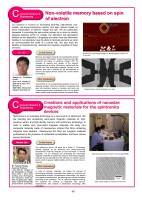
HaeiwaLabSpintronicsisanemergingtechnologyasanewbranchofelectronics.Wearestudyinganddevelopingnano-sizedmagneticmaterialsforhigh-sensitivesensorandhigh-densitymemorywithspintronicstechnology.Inordertorealizesuchnano-sizedmagneticmaterials,Westudynewcompositematerialsmadeofmesoporousorderedthinfilmscontainingmagneticnanoparticles.Mesoporousthinfilmsareinorganicmaterialssynthesizedinthepresenceofsurfactantsastemplates,andhavevariousporousstructures.ThespintronicsdevicewillserveasaGreenITTechnologyproductbecauseofitsdistinctivelowpower-consumingcharacteristicwhilethecomputerisintherest-mode.InHaeiwalaboratory,wearestudyinganddevelopingthenano-sizedmagneticmaterialsforspintronicsdevices.Nano-sizedmagneticmaterialshaveapotentialtobetheultimatenon-volatilememorydevicewhichisspeedy,highlyreliable,andhasalargememory-capacity.Dr.TetsujiHaeiwaAssociateProfessorImetwiththe“magne”atthethird-gradeofcollege.Sincethen,Ihavebeenstudinganddevelopingthemagneticmaterial.Now,I'mgoingalso“Sato-yama”(naturalwoodlands)preservationactivities.Scanning transmission electron microscope(STEM) Creations and applications of nanosizemagnetic materials for the spintronicsdevicesStem photo image of mesoporousthin film.Inordertodevelopmaterials,werepeattheprocessofsynthesizingmaterials,evaluatingthembasedonstructuralandcompositionalanalysis,microstructuralobservation,andelectricandmagneticmeasurement,andalteringthesyntheticconditionsaccordingtotheevaluation.Thisisagenuineengineertraining.Ourstudentsareworkingasengineerswithvacuum,measurement,andanalysis&observationtechnologyaftergraduation.20nmComputerScience &EngineeringAfter GraduationIn the FutureNon-volatile memory based on spin of electronOurresearchisfocusedondevelopingultra-fast,high-density,non-volatile,low-power-consumingmemoryandlogicdevicesbasedondirectmanipulationofelectronchargeandspin.Weareparticularlyinterestedincontrollingthespinseitherpointedupordownbydirectlyapplyingelectricalcurrentorvoltage.Ourlaboratoryhasspecializedfacilitiesforfilmdeposition.Lithographyandothernano-sizefabricationfacilitiesinourlaboratoryhavetheabilitytofabricateelementsassmallasone-thousandththewidthofahumanhair.Wealsohavethefacilitiestocharacterizetheelectricalandmagneticpropertiesofthoseelements.Memoryandlogicalelementsarefundamentaldevicesforprocessinginformation.Currentmemoriesandlogicelementsarebasedonelectricalcharge.Withtheincreaseofcapacityanddensityofthedevices,leakagebecameanissue.Spintronicsexploitsboththeintrinsicspinandassociatedmagneticmomentofanelectron,andhasapotentialforthedevelopmentofmemoryandlogicaldevicesbeyondthecurrentCOMStechnologies.Around50%ofourundergraduatestudentsmovedontograduateschools.Someareworkingincompaniesthatdealwithelectronicsystemordevices,andsomeareworkingasgovernmentemployees,et.al.Itisourgoaltofostercreativeandexcellentstudentswithglobalminds.Xiaoxi LiuProfessorProfile:2013~ Prof., ShinshuU;2003~2012, Asso. Prof. ShinshuU;2002~2003, Researcher, Glasgow Uiversity, UKAtomicforcemicroscopyimagesofnanolithographycarriedoutinourLab.TypicalmemorycircuitpreparedinourLab.写真サイズ高さ4.35cm×幅7.5cm配置位置横11.4cm、縦8.15cmComputerScience &EngineeringAfter GraduationIn the FutureLiuLab48
元のページ