Engineering-Research-Activity2015|SHINSHU UNIV.
23/75
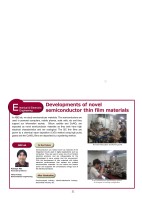
ABE LabElectrical& ElectronicEngineeringInABElab,westudysemiconductormaterials.Thesemiconductorsareusedinpersonalcomputers,mobilephones,solarcells,etcandtheysupportourinformationsociety.SiliconcarbideandCuAlO2areexpectedasnovelsemiconductormaterialsastheybothhavehighelectricalcharacteristicsandareecological.TheSiCthinfilmsaregrownbyachemicalvapordeposition(CVD)methodusinghighpuritygasesandtheCuAlO2filmsaredepositedbyasputteringmethod.Semiconductorsarewidelyknownasmaterialsoftheintegratedcircuitsusedindigitalapplicationssuchascomputers.Theyareusedineveryoneofourfamiliarelectricalproducts,andareindispensableforthetechnologiestosaveenergyandtheenvironment.Withthedevelopmentofnewmaterialswithhigherelectricalperformancesthatreplacethepresentsemiconductormaterials,wecanreducetheelectricpowerandsuppresstheunnecessaryenergylossoftheelectricalproducts.KatsuyaAbeAssociateprofessorFieldofstudySemiconductorengineeringHot-wire CVD system for SiC film growth.Developments of novel semiconductor thin film materialsX-ray photoelectron spectroscopy systemfor analysis of bonding configuration.Semiconductorindustry,electric/electronicsindustry,automobileindustry,etc.In the FutureAfter Graduation21
元のページ